- A - B - C
- D - E - F - G
- H - I - J - K
- L - M - N - O
- P - Q - R
- S - T - U
- V - W - X - Y - Z
- System of Units
- Microelectronics Industry
- Type of component
- ATE:
- Automatic Test Equipment.
- Balanced Contact Force:
- Measured as a « ±% » BCF is the allowable deviation from the floating average contact force.
- Beam length:
- The distance, measure horizontally, from the center of the probe tip to the point the probe enters the epoxy.
- Blade card:
- Probe card that uses ceramic or metallic blades.
- Bond Pad:
- The metalized locations on an integrated circuit where the test probes will make contact.
- Bond Pad Pitch:
- The distance between adjacent bond pad centers.
- Bond Pad Size:
- The measurement of that portion of the bond pad metalization that’s usable for probing.
- Burst Current:
- A current pulse of less than 10ms duration.
- Contact Force:
- The force presented by a probe at overdrive on a bond pad or bump, measured in grams/mil of overdrive (OD).
- Contact Resistance:
- The resistance that occurs at the junction between the probe tip and the device contact surface metalization.
- Dielectric Constant:
- A measure of the ability of the material to resist the formation of an electric field within it.
- Die:
- A single square or rectangular piece of semiconductor material onto which a specific electrical circuit has been fabricated also called a ship or Dut.
- Edge Sensor:
- An edge sensor (E/S) is a two–wire or three-wire probe configuration that forms a switch to detect contact with the wafer.
- EWLP:
- Embedded Wafer Level Packaging.
- Fab-lite:
- Any semiconductor company that out sources less than 75% of it’s wafer manufacturing and is a silicon provider.
- Fabless:
- Any semiconductor company that out sources 75% or greater of its wafer manufacturing and sells silicon to an end-customer.
- Fanout Angle:
- The angle made by a probe with respect to the side of the die, measured from the perpendicular to the die side.
- Floating Average:
- A range of acceptable average values. Applies specifically to contact force.
- FPD:
- Flat Panel Discret Packaging.
- FR4:
- A PCB material.
- FWLT:
- Full Wafer Level Test.
- Glassivation:
- Passivation using silicon dioxide as the coating.
- IDM:
- Any integrated device manufacturer that produces 75% of their silicon internally.
- Leakage Current:
- Parasitic loss of current in an electrical circuit.
- Mask:
- A patterned screen, usually of glass, used to allow exposure of selected areas of photoresist-coated wafer by a light source.
- Measure THD:
- Total Harmonic Distortion.
- Micron:
- A metric unit linear measure that equals on millionth of a meter. Same as micrometer (mm); equal to 25,4 µm.
- Mil:
- One Thousandth of an Inch. Equal to 25,4 microns.
- MotherBoard:
- Tool measure probe card.
- Needle:
- Probe.
- OHM (Ω):
- Unit of measurement used for resistance.
- Overdrive:
- Z axis (vertical) distance measurement calculated from the first contact point of the probe to the device surface.
- Passivation:
- A protective coating placed on a wafer surface. Sometimes called glassivation.
- PCB:
- Printed Circuit Board.
- PCB Aperture:
- A hole opened in the center of the pcb to support attachment ring.
- Planarization:
- The ideal probing operation would result in simultaneous contact of all test pads on each and every device across the substrate.
- Polyimide:
- A PCB material that used for probe cards designed for probing temperatures greater than 100°C.
- Probe Angle:
- The angle of the probe shank where it passes through the epoxy relative to the horizontal plane of the PCB.
- Probe Card Analyzer:
- A piece of test equipment used to measure critical probe card parameters.
- Probe Shank:
- The portion of the probe that isn’t tapered.
- Probe Solder Point:
- The location on the PCB where the probe tail is connected.
- Probe Stability:
- The ability of a probe to retain its performance characteristics over time.
- Probe Tail:
- The portion of a probe outside the ring.
- Probe Tip Alignment:
- Probe tip placement at overdrive with respect to the targets on a coordinates glass mask or bond pads on a wafer.
- Probe Tip Depth:
- The distance from the reference plane of a probe card to the plane formed by the probe tips. This is typically measured from the bottom of the pcb to the probe.
- Probe Tip Length:
- The Vertical distance from the tip of the probe to the bend in the probe.
- Probe Tip Shape:
- The contour of the probe tip; typically flat or radiused.
- Probe Tip Diameter:
- The diameter of the wire material from which the finished probe is made.
- Probing:
- A term used to describe the electrical testing that employs very finely tipped probes applied sequentially to a wafer.
- Raidissor:
- Mechanical part above the spider.
- Ring:
- A ceramic or metallic piece machined to proper dimensions to support probes on a PCB.
- Ring Aperture:
- The opening (hole) in the center of the ring.
- Scrub Mark:
- Mark on the contact surface created by scrubbing action as the probe tip moves across the device metalization when over drive is applied.
- SNR:
- Signal to Noise Ratio.
- Spider:
- Assemby ring with needles.
- Stiffener:
- Mechanical part above the PCB.
- Target:
- A shape on a glass mask that represents the final position of the probe tip.
- Tip length:
- Probe tip length is measured from the tip of the probe to the bend in the probe.
- Touchdown:
- The point of initial contact between probe and bond pad. The number of times the probe card is overdriven onto a wafer during the lifetime of the probe card.
- Wafer:
- A thin disk of semiconducting material on which many separate circuits can be fabricated and then cut into individual ICs.
- WLBI:
- Wafer Level Burn In.
- WLCSP:
- Wafer Level Chip Size Package.
- WLT:
- Wafer Level Test.
- Yield:
- The number of acceptable units produced compared to the maximum number.
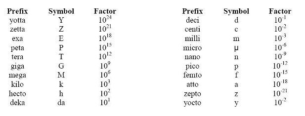
International System of Units
The 20 SI prefixes used to from decimal multiples and sub-multiples of SI units are shown here:
Length measurements
| Unit | Symbol | Equivalence |
| mil | 0.0254 mm | |
| inch | in. or '' | 2.54 cm |
| foot (=12'') | ft or ' | 30.48 cm |
| yard (=3') | yd | 91.44 cm |
| mile (=1760 yd) | 1609 m |
Surface measurements
| Unit | Symbol | Equivalence |
| square inch | sq. in. | 6.45 cm² |
| square foot | sq. ft. | 0.0929 m² |
| square yard | sq. yd. | 0.83 m² |
| square mile | sq. mi. | 2.59 km² |
Volume measurements
| Unit | Symbol | Equivalence |
| cubic inch | cu. in. | 16.39 cm³ |
| cubic foot | cu. ft. | 28.32 dm³ |
| cubic yard | cu. yd. | 0.7646 m² |
Capacitance measurements
| Unit | Symbol | Equivalence |
| English | ||
| pint | pt | 0.568 l |
| quart (=2 pt) | qt | 1.136 l |
| gallon (=4 qt) | gl | 4.545 l |
| American | ||
| pint | US pt | 0.473 l |
| quart (=2 pt) | US qt | 0.946 l |
| gallon (=4 qt) | US gl | 3.785 l |
Weight measurements
| Unit | Symbol | Equivalence |
| Common (English, American) | ||
| ounce | oz | 28.35 g |
| pound (=16 oz) | lb | 0.454 kg |
| English | ||
| hundredweight (=112 lb) | cwt | 50.8 kg |
| British ton or long ton (=20 cwt) | ton | 1,016 kg |
| American | ||
| cental or US hundredweight (=100 lb) | cwt | 45.4 kg |
| US ton or short ton (=20 cwt) | ton | 907.2 kg |
Surface pressure measurements
| Unit | Symbol | Equivalence |
| Pound/Square Inch | PSI | 0.07 kg/cm² |
| pound/square foot | lb/sq ft | 4.88 kg/m² |
Microelectronics Industry
International Electrotechnical Commission |
www.iec.ch | |||
Japan Electronics and Information Technology Industries Association |
www.jeita.or.jp | |||
International Organization for Standardization |
www.iso.org | |||
Korea Semiconductor Industry Association |
www.ksia.or.kr | |||
Semiconductor Industry Association |
www.sia-online.org | |||
World Economic Forum |
www.weforum.org | |||
European Committee for Standardization |
www.cen.eu | |||
European Committee for Electrotechnical Standardization |
www.cenelec.eu | |||
European Electronic Component Manufacturers Association |
www.eeca.eu | |||
European Telecommunication Standards Institute |
www.etsi.org | |||
The European Engineering Industries Association |
www.orgalime.org | |||
The Confederation of European Business |
www.businesseurope.eu | |||
Association Française de Normalisation |
www.afnor.org | |||
National Coordination in Micro- and nanoelectronics Training |
www.cnfm.fr | |||
Filières des Industries Electroniques et Numériques |
www.fien.fr | |||
Groupement des Fournisseurs de l'Industrie Electronique |
www.gfie.fr | |||
Groupement des Industries de l’interconnexion, des Composants et des sous-ensembles Electroniques |
www.gixel.fr | |||
Syndicat de l'Instrumentation de Mesure, du Test et de la Conversion d'Energie dans le domaine de l’électronique |
www.simtec.org | |||
Syndicat Pofessionnel de la Distribution en Electronique Industrielle |
www.spdei.fr | |||
Syndicat professionnel des fabricantsde fils et Câbles Electriques |
www.sycabel.com | |||
Union Technique de l'Electricité |
www.ute-fr.com |
Type of component
BCC : Bump Chip Carrier |
www.wikipedia.org | |||
BGA : Ball Grid Array |
www.wikipedia.org | |||
LCC : Leadless Chip Carriers |
www.wikipedia.org | |||
LDFP : Low Profile Quad Flat Package |
www.wikipedia.org | |||
LGA : Land Grid Array |
www.wikipedia.org | |||
MLF : Microlead Frame |
www.wikipedia.org | |||
PBGA : Plastic Ball Grid Array |
www.wikipedia.org | |||
PGA : Pin Grid Array |
www.wikipedia.org | |||
PLCC : Plastic Leaded Chip Carrier |
www.wikipedia.org | |||
QFN : Quad Flat No Leads |
www.wikipedia.org | |||
QFP/MLF : Quad Flat Package |
www.wikipedia.org | |||
SOIC/SO : Small Outline Integrated Circuit |
www.wikipedia.org | |||
TQFP : Thin Quad Flat Pack |
www.wikipedia.org |